
A PCB is a magical thing that transforms a pile of components into smart devices (to do this we still need the right incantation in the form of uploaded firmware). A PCB is an essential layered skeleton that creates functional connections between electronic components.
A PCB consists of multiple layers, typically using composite materials - resins filled with glass fibers of varying density as insulators/interlayer dielectrics. Also, other special materials may be used like ceramics, Teflon, or some plastics.
PCB Structure
- Base Layer: The base layer of the PCB is an insulating material that provides mechanical strength to the board. Fiberglass (FR-4) is most commonly used for its affordability, mechanical strength, and thermal stability. Ceramic or flexible substrates may be designed for special applications.
- Conductive Layers: Copper foil forms the conductive layers on the surface or inside the board. These layers are interconnected by plated-through holes (VIAs) that enable signal transmission between layers.
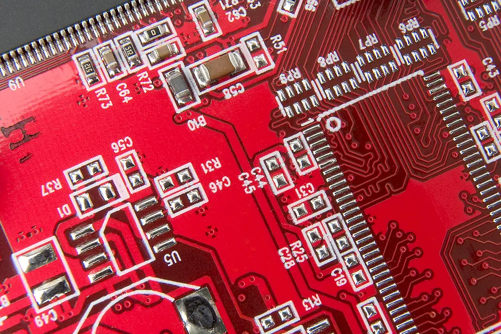
- Surface Finish: The PCB surface combines two distinct areas: solderable pads with surface finishes (using Gold, Silver, or other alloys) and a surface surrounding them.
- Solder Mask: The non-solderable surface of the PCB is covered with a solder mask, an insulating layer that protects the copper paths from oxidation. It provides basic circuit protection, functional coverage, appearance, and a surface for future printing. While typically green, other colors can be preferred in specific cases.
- Silkscreen: Labels, symbols, and component markings are silkscreened on the PCB to facilitate assembly and diagnostics.
- to facilitate assembly and diagnostics.
Types of PCBs
- Single-Layer PCB: A specialized solution, particularly notable in the single-layer on thermalclad variant designed for applications with high power losses.
- Double-Layer PCB: Features copper on both sides of the substrate. Particularly important in mass production series and automotive applications.
- Multilayer PCB: Consists of several copper layers separated by insulating layers. These boards enable the implementation of complex circuits in a compact format. Due to increasing EMI suppression requirements, most modern devices, now use multilayer boards (4 or more layers).
- Flexible and Rigid-Flexible PCB: Flexible PCBs use materials that allow bending and shape adaptation. Rigid-flex PCBs combine rigid and flexible parts, enabling their use in complex mechanical assemblies.

PCB Manufacturing Process
- Design: The PCB is designed using CAD software (e.g., OrCAD (our primary tool), Altium Designer, Eagle, KiCAD), where schematics and board layouts are created.
- Etching: The copper foil is covered with photoresist, exposed, and developed to create the pattern of paths. Etching follows, where unprotected copper is removed with acid or alkali.
- Stacking and Laminating: Essential for multilayer boards, which are now standard in most electronic devices due to EMI requirements. Even relatively simple devices like automotive lighting systems now commonly use 4-layer PCBs.
- Drilling and Via Formation: CNC machines drill holes for components, while lasers create micro vias. Both types of holes become plated-through holes (VIA) after plating.
- Plating: The holes are coated with copper to create electrical connections between layers. For advanced ELIC (Every Layer Interconnection) technology, the process requires multiple iterations by returning to step 3 to repeat the stacking and plating stages.
- Applying Mask: The solder mask is applied to provide basic circuit protection, functional coverage, and create a surface suitable for printing.
- Surface Finishing: Exposed copper is covered by a conductive and solderable layer, which can be Gold, Silver, or different alloys like ENEPIG. In RF applications, the surface finish is crucial for final performance parameters.
- Silkscreen: Labels, symbols, legends, and component markings to facilitate assembly are printed on the PCB.
- Assembly and Depanelization: PCB boards remain part of a larger panel during the assembly process, enabling more efficient production. The assembly itself is a complex process including washing, solder paste application, component placement, soldering, inspections, bonding, next inspections, and conformal coating. This is followed by depanelization - separation of individual boards from the panel by cutting or breaking, and final testing. Panel-based manufacturing allows for more efficient handling, better utilization of production equipment.
Applications of PCBs
PCBs are indispensable in most modern electronic devices, from simple devices like clocks or calculators to complex systems (computers, mobile phones, medical devices, industrial machines, and military equipment).

External resources
IPC - Association Connecting Electronics Industries — An international organization providing standards, training, and resources for PCB manufacturing and design.
NextPCB Blog — A blog with a wide range of information and tutorials on PCB design and manufacturing.
EDN Network — A website focused on electronic design. You can find articles, tutorials, and news in electronics and PCBs.
All About Circuits — A community platform for engineers and electronics enthusiasts, offering tutorials, articles, and discussion forums.